Lightspeed India Leads 9 Million Dollar Seed Round In Discovered Materials: AI Agents For Cooler Chips And Faster Materials Discovery
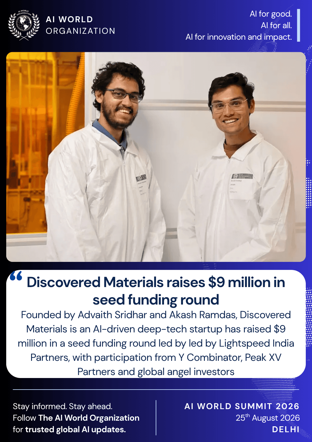
Discovered Materials, a San Francisco-based deep-tech startup, is trying to break that bottleneck with AI. The company has just raised 9 million dollars in seed funding, in a round led by Lightspeed India Partners, with participation from Y Combinator, Peak XV Partners, and angel investors including Paul Graham, Gokul Rajaram, and Thariq Shihipar. For an early-stage company that only emerged from Y Combinator’s Spring 2026 batch, this round marks a strong vote of confidence in agentic AI applied to materials discovery.
Introduction
Progress in semiconductors has always depended on new materials. Every major jump in performance or efficiency – from silicon to high-k dielectrics to advanced interconnects – started with years of lab work, simulations, and testing. That timeline is now colliding with AI’s demand for compute. As model sizes grow and data centers expand, chips are hitting power and heat limits faster than materials science can keep up.
What Discovered Materials Is Building
Discovered Materials describes itself as a company building AI agents that discover and accelerate the adoption of new materials for semiconductor chips. Instead of relying only on traditional simulation plus lab experimentation, it uses swarms of autonomous “AI scientists” that explore combinations of elements and structures, model their properties with physics-informed machine learning, and prioritize promising candidates.
The goal is straightforward but ambitious: compress materials R&D timelines from a decade to months. Today, finding a new material that works in chips involves countless iterations: hypothesize, simulate, fabricate, test, iterate, scale, and integrate. Discovered Materials wants its agents to handle many of those loops in silico, surfacing candidate materials that are far more likely to survive real-world testing.
Lightspeed partner Hemant Mohapatra compared the approach to “playing whack-a-mole with atomic structures,” with AI agents continually trying different configurations in search of better thermal and electrical performance. That metaphor captures the core idea. The agents can explore vast chemical spaces far faster than human teams, narrowing down options before the lab gets involved.
The Funding Round And Backers
The seed round is 9 million dollars (around ₹75–85 crore) and is led by Lightspeed India Partners. Participation includes:
Y Combinator, which backed Discovered Materials in its Spring 2026 cohort;
Peak XV Partners, one of India’s largest venture firms with deep experience in global tech;
Angel investors Paul Graham, Gokul Rajaram, and Thariq Shihipar, all known for backing high-leverage technical founders.
For Lightspeed India, this is another bet on vertical AI in a deep-tech domain. For Y Combinator and Peak XV, it is a continuation of a thesis that agentic AI can transform capital- and knowledge-intensive industries like semiconductors.
Releasing New Materials And A Benchmark
Alongside the funding announcement, Discovered Materials has released hundreds of new materials discovered by its frontier AI models plus Material Discovery Bench, described as the first benchmark for agentic materials discovery on real-world semiconductor problems.
Material Discovery Bench is important for two reasons:
It provides a way to compare different AI approaches on realistic constraints (thermal limits, manufacturing compatibility, cost).
It acts as a reference point for how “AI scientists” should be evaluated beyond toy datasets or purely academic metrics.
By publishing both materials and a benchmark, Discovered Materials is signaling that it wants to be part of a broader ecosystem, not a closed black box.
Why This Matters For Semiconductors And AI Compute
Semiconductors are at the center of the AI economy. As models grow, data center energy use and cooling requirements are becoming critical bottlenecks. Better materials for interconnects, heat spreaders, dielectrics, and packaging could directly translate into more efficient chips, lower power consumption, and improved performance per watt.
Discovered Materials is attacking this from the angle of materials discovery. Its agents aim to identify:
Materials that conduct heat more efficiently to cool chips.
Materials that reduce electrical resistance in interconnects, lowering energy loss.
Materials compatible with advanced process nodes and packaging technologies.
If successful, the platform could become an upstream enabler for chipmakers, helping them incorporate new materials into products faster than traditional lab-heavy pipelines would allow.
It is also an example of how agentic AI is moving into hard science domains, not just content, code, or marketing. Agentic materials discovery requires:
Coupling AI agents with physics-informed models and domain-specific constraints.
Integrating with lab workflows and experimental validation.
Managing IP, licensing, and collaboration with industry partners.
This is the kind of multi-layered environment The AI World Organization is particularly interested in tracking.
How Discovered Materials Plans To Use The Funding
According to the company and multiple funding reports, the 9 million dollars will be used to:
Expand the team, hiring more AI researchers, materials scientists, and engineers.
Grow lab capacity, bridging the gap between AI-generated candidates and physical testing.
Scale the AI research agents, enabling more parallel exploration and refinement.
There are also indications that Discovered Materials plans to patent promising materials and license them to chipmakers, positioning itself as both a technology and IP company. That dual role – platform and material IP holder – could be powerful if its discoveries prove commercially viable.
Opportunities And Challenges Ahead
The opportunity is clear. If Discovered Materials can consistently find materials that meet semiconductor industry constraints and pass lab validation, it could:
become a key partner for major chipmakers and fabs,
accelerate innovation cycles in cooling, interconnects, and packaging,
and contribute to closing the gap between AI’s demand for compute and the hardware’s ability to deliver it.
However, the challenges are equally significant.
First, materials science is unforgiving. Many promising candidates fail when scaled or integrated into complex systems. Discovered Materials’ agents must be tightly coupled with physical validation and process-aware models to avoid chasing dead ends.
Second, qualification timelines and manufacturing constraints can still be long, even if discovery is faster. Collaborating with foundries and OEMs, navigating reliability standards, and ensuring supply chain viability will be crucial.
Third, IP and collaboration models need careful design. Balancing open benchmarks with proprietary discoveries and aligning incentives between Discovered Materials and its partners will shape how broadly the platform is adopted.
Finally, there is the broader question of trust in AI-generated science. While AI can accelerate exploration, stakeholders will demand transparency in methods, assumptions, and limitations. The released benchmark is a good starting point, but sustained credibility will require ongoing validation.
What This Means For AI And Deep Tech Funding
From The AI World Organization’s perspective, Discovered Materials’ raise highlights several trends in AI and deep tech funding:
Investors are increasingly backing vertical, agentic AI platforms that operate in capital-heavy industries like semiconductors, energy, and materials, not just in software.
Seed rounds in deep tech sectors are getting larger, reflecting the need to build both software and physical infrastructure (labs, testing rigs, hardware).
Founders with strong technical and domain backgrounds, like Discovered Materials’ team, are attracting support from both global and India-focused funds.
It also underscores the growing importance of AI for scientific discovery, a space that includes protein folding, drug design, climate modeling, and now, materials science. As these platforms mature, they will reshape not just how we build models, but what hardware and physical systems those models run on.
Closing Thoughts
Discovered Materials’ 9 million dollar seed round, led by Lightspeed India Partners, marks a notable moment at the intersection of AI and semiconductors. It is a bet that swarms of AI agents can help discover and validate new materials for chips fast enough to keep pace with the AI boom.
If the company can turn its “AI scientists” into reliable engines of discovery and build strong bridges to fabs and chipmakers, it will become one of the key players defining how AI accelerates physical innovation, not just digital output.
For now, it is a compelling example of where deep-tech funding is headed: toward platforms that tackle real-world constraints with AI, and toward founders who see scientific discovery as a domain where AI can contribute meaningfully rather than just automate tasks.